RXV: RISC-V RV32IMA CPU
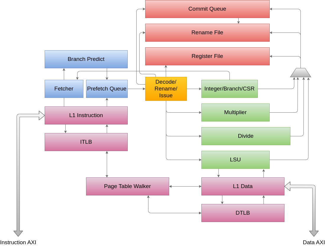
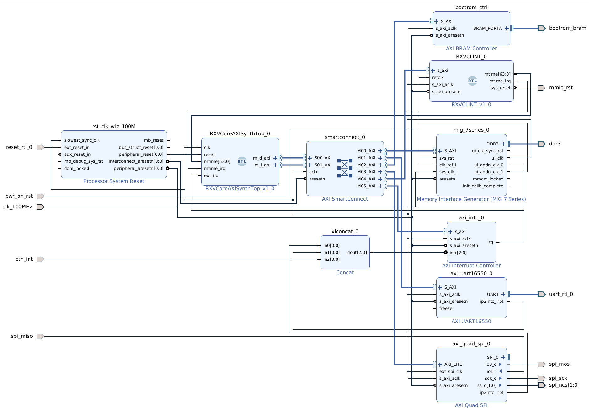
The RXV core is an Apache 2.0 licensed RISC-V RV32IMA CPU that successfully runs mainline Linux with a CoreMark score of 2.61/MHz. The core is in-order with a 7 stage pipeline, out of order completion, register renaming, dynamic branch prediction and indirect branch target prediction, set-associative caches, fully associative TLBs and AXI4 support. A design for the Digilent Arty S7 board uses 32KB 8-way associated cache and 16 way fully associative TLB each for instruction and data paths. Externally, Xilinx IP provides AXI4 interconnect, SPI controller, interrupt controller, DDR3 controller and 16550A.
On top of the RV32IMA base, the following extensions are implemented:
- Zicsr
- Cifencei
- Sstc
- Sscofpmf
The pipeline consists of:
- Fetch 1: next PC generation, combined BTB/PHT lookup
- Fetch 2: instruction cache tag lookup, instruction TLB lookup, branch prediction resteer
- Fetch 2: tag compare, prefetch queue write
- Decode: instruction decode, register rename, misidentified branch resteer and issue. All instructions apart from atomic fetch/op/store are a single uop, atomic operations may require more than one uop
- Execute: execute in one of 4 functional units:
- LSU: fully pipelined 3 cycle load-use latency. Misaligned load/store exceptions are raised in the first cycle, invalid AMO (atomic to device memory) and page faults are handled in the second cycle
- Integer: integer operations, branches, CSR accesses, 1 cycle latency with result forwarding back to input. Illegal instruction, branch alignment and environment call exceptions are raised here
- Multiply: fully pipelined 5 cycle result-use latency
- Divide: non-pipelined 33 cycle result-use latency
- Writeback: results are written back to the register file
- Commit: rename file updated and exceptions raised
Atomic operations are broken down into multiple micro-ops using register rename.
Performance Counters
There are a configurable number of performance counters in addition to the mcycle+minstret fixed counters which can be used for profiling:
- PMU_CYCLES
- PMU_INSTRET
- PMU_BRANCH
- PMU_BRANCH_MISPRED
- PMU_FE_STALL
- PMU_BE_STALL
- PMU_L1D_READ
- PMU_L1D_READ_MISS
- PMU_L1D_WRITE
- PMU_L1D_WRITE_MISS
- PMU_L1I_READ
- PMU_L1I_READ_MISS
- PMU_DTLB_READ
- PMU_DTLB_READ_MISS
- PMU_ITLB_READ
- PMU_ITLB_READ_MISS
FPGA Implementation
The default Arty S7 configuration has:
- RXV Core
- 32KB 8-way set associated instruction cache
- 32KB 8-way set associated data cache
- 16-way fully associated instruction TLB
- 16-way fully associated data TLB
- MTIME reference at ~10MHz
- Separate AXI4 instruction+data busses
- Xilinx AXI interrupt controller
- Xilinx AXI 16550A UART
- Xilinx AXI SPI master with 1 chip select and 256 byte FIFO
- Xilinx AXI4 SmartConnect
- Xilinx AXI memory adapter connecting to the BootROM
The bootrom fetches the generic platform build of OpenSBI and a flattened device tree from a FAT partition on the micro SD along with a gzip compressed Linux kernel before transferring control to OpenSBI.