S80186: 16-bit 80186 compatible core
The S80186 core is a compact, 80186 binary compatible core, implementing the full 80186 ISA suitable for integration into FPGA/ASIC designs. The core executes most instructions in far fewer cycles than the original Intel 8086, and in many cases, fewer cycles than the 80286. The core is supplied as synthesizable SystemVerilog, along with a C++ reference model, extensive tests, a reference BIOS implementation and reference FPGA designs. The core is released under the GPLv3 license.
The 80186 core has also been implemented in an 8088 pin compatible module to accelerate an IBM PC XT compatible system.
Get the source from GitHub.
Features
- Binary compatible with the Intel 80186 core
- MS-DOS
- FreeDOS
- OpenWatcom/GCC ia16-elf compilers
- Separate data/IO and instruction busses
- 1MB addressable segmented memory
- 64KB addressable IO space
- Lock signal for atomic accesses
- 256 external interrupts
- 1 non-maskable interrupt
- 3 stage fetch/decode/execute pipeline
- Debug interface suitable
- JTAG TAP compatible
- Register/Memory access
- Execution control
- FPGA builds (Intel Cyclone V)
- 60MHz FMax
- ~1800 ALMs
Implementation
- Full synthesizable SystemVerilog
- C++ reference model
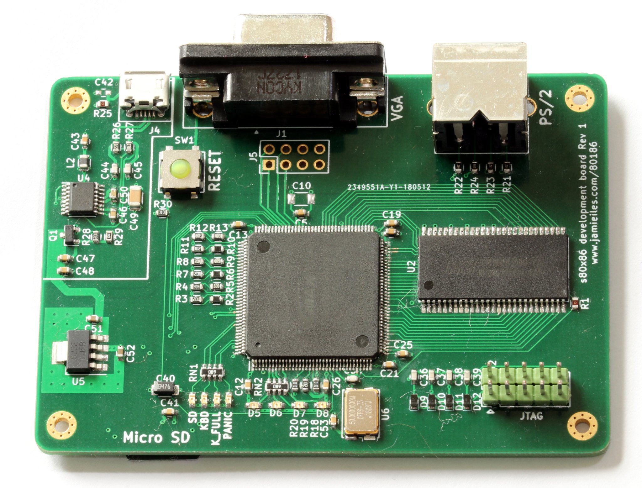
- FPGA reference designs for Terasic DE0-Nano and DE0-CV
- Extensive test suite verified against C++ model, RTL and FPGA
- Complete Docker build environments
- Full development documentation and programmers guide
Reference Design
- SDR SDRAM controller
- SD card for fixed disk emulation
- 8259 PIC-lite controller
- UART
- 8254 PIT-lite timer operating in mode 2 only.
- CGA controller with VGA output
- PS/2 controller with keyboard and mouse support
- 8KB direct mapped cache for SDRAM accesses


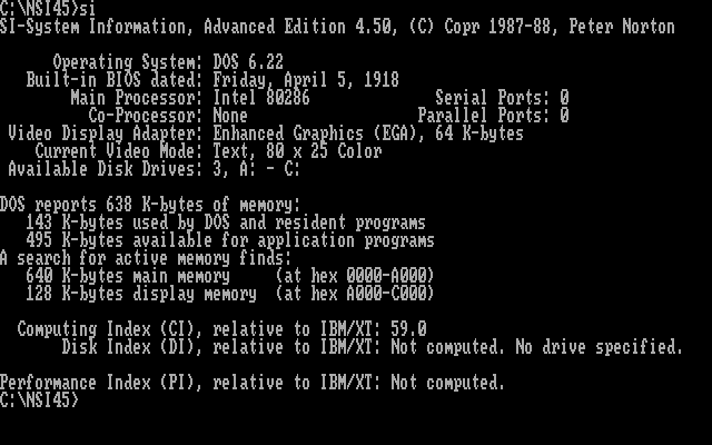
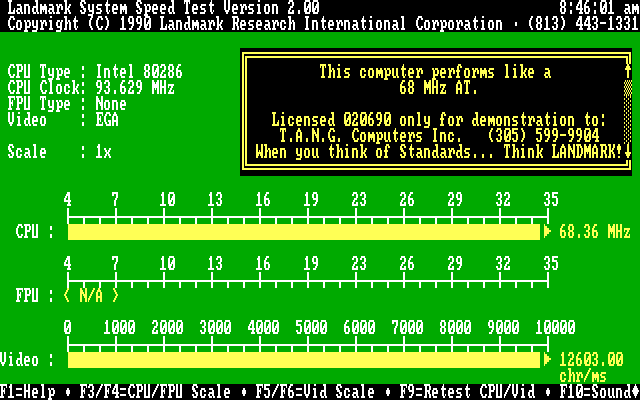
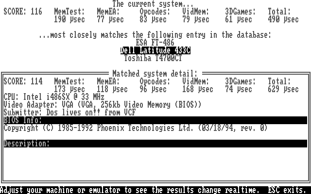
Note: all images captured on real hardware from the VGA frame buffer.
Architecture
The S80186 is a 16-bit architecture with 8 16-bit general purpose registers, 4 segment registers allowing access to 1MB of physical memory. The architecture uses a variable length instruction encoding allowing for high code density. The core is a microcoded design using a small amount of logic and a flexible microassembler. The microsequencer is used to implement an efficient debug interface that can be connected to a JTAG TAP or disabled if required.
Full compatibility with 80186 ISA is provided, implementing all instructions, traps, faults and interrupts and known errata. Undocumented instructions such as SETALC are also implemented.
Software
The S80186 core is compatible with the Intel 80186 and so enjoys extensive software compatibility. There are a wide range of development tools available including OpenWatcom, GCC and NASM, and the core can run existing operating systems such as MS-DOS and FreeDOS. A sample BIOS implementation is provided for the FPGA designs.
Downloads
| Download | Version | Signature |
|---|---|---|
| DE0-CV SRAM Object File | 20180307 | GPG Signature |
| Development Guide | 20180307 | GPG Signature |
| FreeDOS SD card image | 20171106 | GPG Signature |
| Source release | 20180307 | GPG Signature |